Technology
Electron-beam lithography and proximity effects
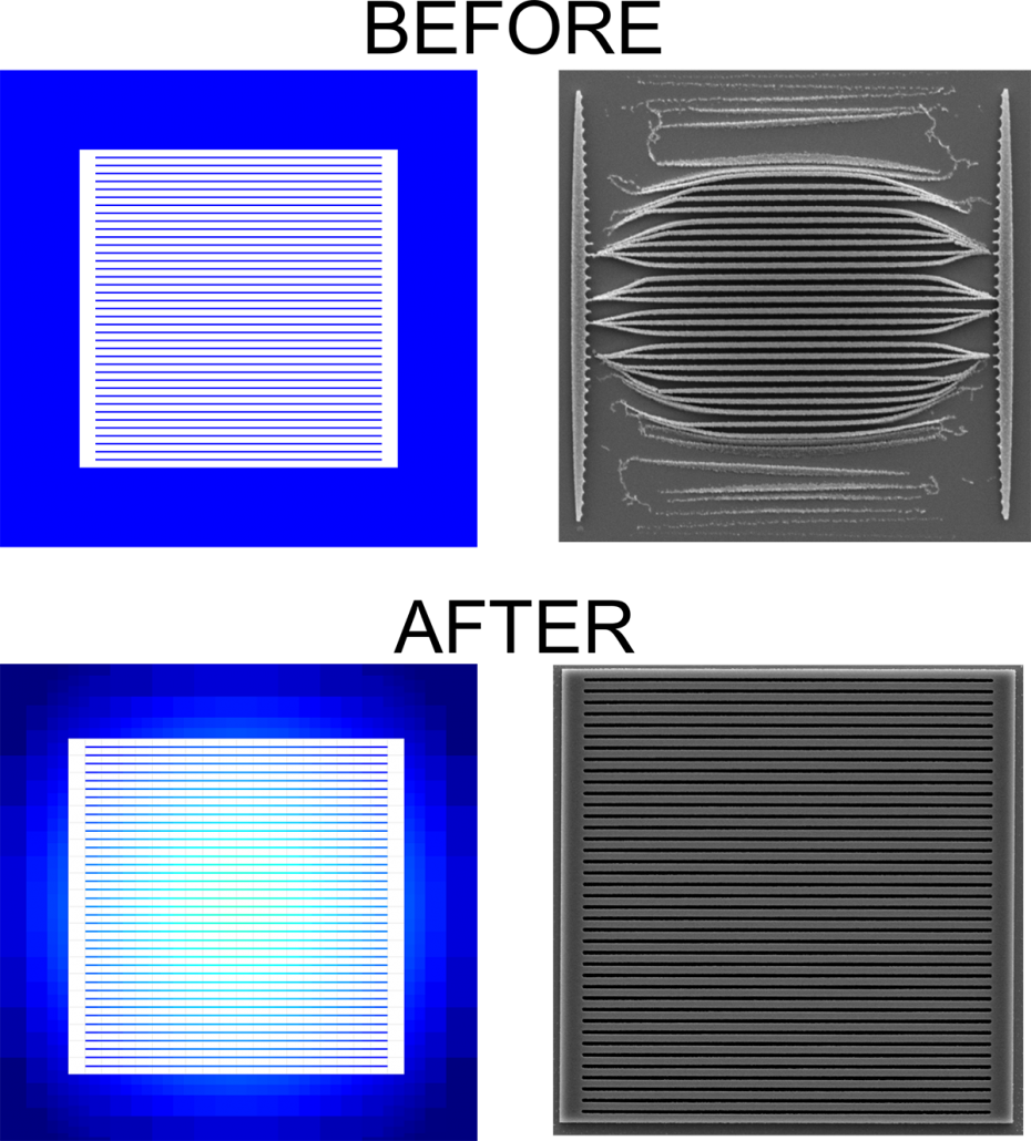
Electron-beam lithography is the state-of-the-art method for high-resolution nanofabrication. With an electron beam waist of less than a nanometer, intricate nanoscale patterns can be written in electron-sensitive resists. Unfortunately, the electrons scatter off the resist and the substrate, which results in unwanted exposures known as proximity effect errors. An example is a grating within an exposed region as shown to the right. If a constant exposure time is applied (BEFORE, blue region), the actual electron dose varies dramatically across the device and the result shown in the SEM image shows detrimental device failure.
Enter Beamfox Proximity. Our software calculates the electron trajectories and our advanced algorithms corrects the exposure times. The result is shown with the bottom images (AFTER, local dose shown by color scale). With Beamfox Proximity, the intended pattern is accurately transferred from design file to the lithography mask. While the difference between before and after might seem subtle at the level of the exposure file shown on the left, the difference is dramatic in the actual devices shown on the right.
This might sound as if Beamfox Proximity is a complex product with a thick manual but in fact it is quite the opposite. Beamfox Proximity was built from the ground up taking the process engineer’s perspective so we wrapped our complex algorithms in a smooth, intuitive, and fast graphical user interface. In short, Beamfox Proximity is proximity error correction made simple. But don’t just take our word for it, download our free trial and see for yourself.


